0512-57906238
Tel:13656269491
Fax:0512-57906239
Mail:mef@micro-ef.com
Addr:No. 189, ZhangJi Road Kunshan City ,China
High Precise Stencil for Wafer Bumping process
Product introduction
4 ~12 inch wafer bump package ball template
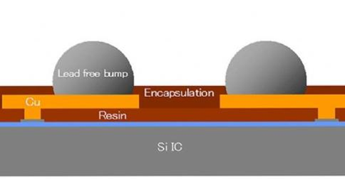
IC plate, PAD bump package, implant template
The ball diameter is 50 ~ 350um
It covers all package forms such as SIP system package, WLP wafer packaging, FC flip chip and so on
Chip 3D package perfect solution
Use | IC Carrier plate bump package | Wafer chip bump packaging |
manufacturing method | Electroforming(electroforming) | Electroforming(electroforming) |
Texture of material | Ni alloy | Ni alloy |
Maximum template size | 800×800mm | 800×800mm |
Thickness range | 0.02~0.2 mm | 0.02~0.35mm |
Width thickness ratio | 0.02~0.10 → ±0.003mm | 0.02~0.10 → ±0.003mm |
Width thickness ratio | Picture thickness: board thickness=1:1 | Graphic width: board thickness=1:1.5 |
Opening accuracy | Specified value±0.005mm | Specified value±0.005mm |
Length accuracy | ±0.015mm | ±0.015mm |
Graphic film | High precision DPI film | High precision DPI film |
Net frame | Aluminum alloy (hollow) | Cast aluminium, cast iron, heavy aluminum, etc. |
Tension | 1.0~1.2mm ※STG-75Determination of value | 0.75~0.80mm ※STG-75Determination of value |


