0512-57906238
Tel:13656269491
Fax:0512-57906239
Mail:mef@micro-ef.com
Addr:No. 189, ZhangJi Road Kunshan City ,China
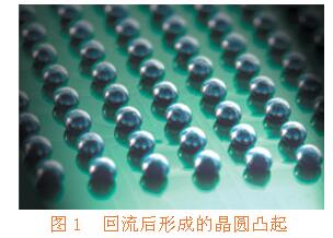
At present, there are several technologies available for coating solder paste on wafer pads. This technique is called wafer bumping technology. The use of halftone printing for wafer bumping is widely accepted as a cost effective mass production solution. However, as the number of I/O increases and the spacing becomes smaller, this method of printing solder paste on the solder joints becomes more challenging, and the requirements of the matching process design level are also greatly improved.

Why stencil printing method?
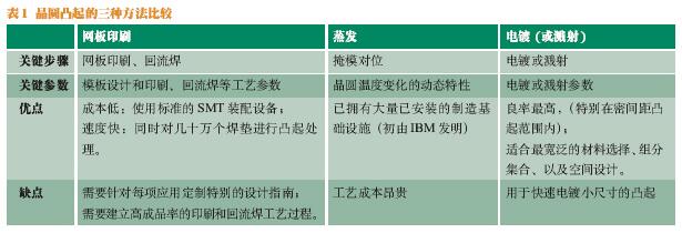
The industry's three most famous wafer projection methods - screen printing, evaporation and sputtering or electroplating - each has its advantages and disadvantages (Table 1). The choice of method, in addition to the company's technology roadmap, the more important is the need to consider many parameters including convex space, convex height, wafer substrate, wafer thickness, wafer size, convex consistency, and raised material.

Equipment and materials
The wafer mount printing method is designed to be compatible with the standard surface mount assembly line tool, so no additional investment is needed to upgrade or retrofit existing large equipment.
The screen press, however, should be equipped with sophisticated optical devices. The alignment system shall be able to identify non-standard reference points on the wafer to be processed, including pads, corners, special marks, markings, or other metallization features contrasting to the background coverings.
In printing, it is necessary to use rigid trays to support wafers in order to ensure the safe handling of precision wafers.
Wafer bumps usually use water-soluble solder paste. Raised must be clean, fluxing treatment later easy flip chip assembly process, in order to achieve stable wetting and consistent bond; in addition, minimizing any residue accumulation between convex or convex, the flip chip assembly after filling the bottom glue more reliable art. Up to now, there is no commercially available non cleaning solder paste for solder joints.
Process steps
Wafer bumping printing
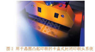
The process is similar to printing on the FR-4 substrate. First, the wafer is placed on a tray, with transfer to screen printing machine through the transfer; then, the scraper printing mode, first paste stir for 30 to 60 seconds, ready for loading, which is uniformly applied flux and solder powder, and solder paste to the appropriate dilution important step consistency, (using the card cassette with automatic perfusion and mix welding function closed print head system, this step can be omitted); then, after applying solder paste to the screen, the video system of printing machine will find all the reference points in the solder paste clean wipe the entire screen surface, the injection hole in all; finally, the tray and the wafer is transferred from a printing press.
Location check
The deposition of the solder paste shall be examined by microscope, and the solder paste shall be properly positioned to cover all the pads. This is the key element to ensure a steady reflow process. For high-density fine pitch configurations, achieving perfect print alignment is a challenging task and sometimes requires manual alignment of offset positions.
Reflow soldering
Once the solder edge check has been completed, the printed wafer can be reflow in the forced convection furnace.
Cleaning and drying
In the cleaning process, wash the wafer with mild deionized water and remove the water-soluble flux. Then dry the wafer with clean forced convection air or nitrogen. Finally, it is recommended that the wafer be dehydrated for two hours at 125 DEG C to remove any moisture that may be absorbed during the wafer cleaning process.
Cleaning screen
The cleanliness of the stencil is also critical. Even after a single printing stroke, the inner wall of the stencil will accumulate a great number of solder paste residues that will soon become dry and stain the subsequent printing stroke.
Process parameters affecting wafer yield
Many variables seriously affect the quality or yield of wafers using this projection method. Known good, die, and KGD are usually used to indicate the performance of the wafer bumping process. The most important factors to be considered for successful wafer printing include solder paste, printing environment (environment and humidity), printing machine settings, reflow soldering status, and cleaning options.
Soldering paste
An important feature of solder paste is particle size and distribution, depending mainly on the amount of solder paste deposition and the size of the stencil opening. It is generally believed that the particle size distribution of solder paste shall allow at least three of the largest solder balls to meet the width of the smallest opening on the board. This is the famous "three ball law"". The distribution and density of solder particles directly affect the rheological properties of solder paste, and also affect its performance on a screen press.
In wafer screen printing, it is best to use the fine solder powder; reported metal content of Sn63/Pb37 type V solder paste particle distribution of up to 90%, can be effectively used for 8 mil spacing pad convex processing, the protruding height reached 5 mil.
Solder paste for wafer printing, whose exposure time and life cycle limit are shorter than the standard values of SMT solder paste. In order to maximize the life cycle of the solder paste, the solder paste should be removed from the screen as long as the printer is idle. An important advantage of using closed transfer systems is that the solder paste is always closed and isolated from the surrounding environment.
temperature and humidity
The main effect of the environment is that moisture is absorbed into components and substrates, especially in solder paste. Compared to non clean solder paste, water-soluble wafer raised solder paste is more sensitive to these environmental changes. If relative humidity levels exceed 60%, moisture will enter the water-soluble solder paste; on the contrary, if the relative humidity is below 40%, it will cause the solder paste to dry prematurely. In either case, the printing performance of the solder paste will be changed, and the stencil printing process will deviate greatly from the normal process, thus becoming the most important link in the assembly process. It is suggested that the temperature should be kept between 21 and 25 degrees Celsius, the relative humidity level should be between 40% and 60%, and the deviation from the set point should be reduced as much as possible.
Printer settings
Screen printing machine now offers a variety of printing pressure, speed and speed of separation, and can choose the number of printing head paste formula and many different equipment modernization, the selection of printing parameters suitable as a not easy work.
The advent of enclosed print heads has brought significant benefits to the wafer bumping process.

Parameters of reflow includes preheating rapid heating with flux reached 150 - 10 Deg. C activation temperature of the platform, then jumped sharply to 220 - 10 Deg. C, higher than the alloy liquid temperature, finally is the rapid cooling stage (which is of Sn63/Pb37 alloy is recommended). During reflow soldering, the residence time of the wafer in each temperature zone is considerable, and the temperature rise / fall rate shall be accurately controlled according to the technical specifications provided by the solder paste supplier.
Remove flux residue
The longer the time interval between reflow and cleaning, the greater the difficulty of removing solder flux.
The successful implementation of screen printing process for wafer bumping needs to improve the requirements of the matching materials (such as solder paste, mesh board, etc.) and the level of process design. In addition, important design parameters include: wafer bumping process design, flip chip bonding pad pad pad spacing and size / shape / position, bump metallization, tray design, screen design, plate thickness, hole size / shape, direction of hole and hole positioning. Only a thorough understanding of the many design strategies that affect the process can achieve remarkable results.