0512-57906238
Tel:13656269491
Fax:0512-57906239
Mail:mef@micro-ef.com
Addr:No. 189, ZhangJi Road Kunshan City ,China
Basic design items that affect the printing effect of wafer bumping screen board
Preface
A number of important design factors must be considered in order to ensure that the wafer to wafer process is satisfactory to a desired level.
Screen Printing
Screen printing technology using standard surface mounting equipment is a cost-effective program for bonding wafer raised pads in simple and mature process conditions. With this method, different applications need different customized design guidelines, and compliance with specific equipment, materials and process instructions, to establish stable and high yield of the wafer bumping printing and reflow process.
Parameters affecting the good rate
Although the screen printing is simple and direct, but many variables will seriously affect the quality of the wafer projection method or yield, usually with numerical known good die (KGD) to evaluate the performance of a wafer bumping process. Should understand and attach great importance to the work of the many effects of art design, in order to get remarkable achievements make design strategy is effective and reliable.
Flip chip bonding pad design
Flip chip bonding, rather than line up chip on board device is one of the advantages, because the conductive pad can be placed on the die surface effectively at any point, it can increase the number of I/O in integrated circuit on a smaller area. However, the print bump may be the most restricted and hindered printing method of the bare sheet pad layout. The size, shape and spacing of the pad must be carefully designed so as to achieve the desired size of the solder paste in actual circumstances; in addition, the bonding surface combinations of pads, which are generally referred to as raised base metal, must also be considered. In reflow process, UBM has a significant effect on the shaping of screen printed solder balls, and ultimately affects the strength, reliability, and performance of the assembled flip chip.
Pad size and shape
The size of the pad on the chip, which raised the reflow solder paste volume required to specify the size of screen printing has a direct impact, to maintain the height of the projection of the specified chip pad, larger need more small pad solder paste solder paste need less. If the pad is too small to support a larger amount of solder paste, the weld area is smaller, and the bump and solder joint strength are significantly affected, while the benefit is only a slight increase in gap distance. The shape of the wetted weld area of the chip pad also affects the projection size of the solder paste. This shape is not necessarily related to the geometry of the pad, but is mainly determined by the passivation hole on the pad (see Figure 1).
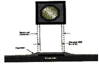
Figure 1: the passive film opening of the pad determines the solder paste
The size and geometry of a raised wetted bond area.
Figure 1 the actual bonding point shape is octagonal, pad is square, the shape defined by the passivation window, all in order to reduce the stress concentration in welding ball base angle of the sea, the stress may weaken the bond strength, and affect the reliability of solder joints. To reduce this condition, circular passivation holes are ideal. However, some wafer fabrication systems have problems in manufacturing round corners with sharp corners.
One experience is to maintain the maximum size of the bonding pad at no more than half of the pitch and minimum no less than 65um (Note 1). To calculate the size of the reflow bump with the size and geometry of the pad, the following equation can be used. The equation simulates a reflow bump, represented as a flat, geometric sphere, and serves as a stencil design tool that helps determine the appropriate stencil perforation size to coat the required solder paste volume.
Solder paste raised volume: {1 / 2 (pad pad area) x (raised height)}+{1 / 6 PI (raised height) 3}
The basic design items that affect the printing effect of wafer bump screen -2
Pad spacing and position
Whether or not stencil printing can produce large solder paste bumps on wafers depends mainly on the configuration and density of the pads. We suggest that the wider the spacing of the pads, the better the flexibility of the design in relation to the shape and location of the perforation, so as to maximize production. The high-density layout can also be more effectively designed to stencil the stencil for larger solder paste, and only the adjacent pads are staggered. It is more challenging to design a mesh board with multiple pad configurations, because the foil surface of the stencil will be filled with holes and become very complicated. At present, the advanced fine pitch screen printing technology seems to remain at the critical point of 6mil, but these boundaries are constantly challenged. Although it can be printed in small spacing condition, but the amount of paste in the flawless case coating is very limited, enough to let the industry set off on the bulge size, clearance, and bottom filling ability, joint strength and reliability of the whole issue.
In terms of the position of the pad, in general, each corner pad on the bare sheet is the most difficult place to achieve consistent and no defects in the amount of printed solder paste. The non standard punch shapes here is necessary, because of the high density perforation may take up a lot of screen area, while the shape of special coating is difficult to predict the perforation transfer efficiency, so the height distribution raised on the die were not satisfied. Only when all the pads on the wafer are removed, this potential problem can be avoided and the design of the stencil perforation is more flexible.
Raised base metal
In reflow, the solder paste metallurgy must be bonded to the solder paste to ensure that the printed solder paste is properly adhered to the wafer pad. Most of the bare pads are made of aluminum and are not bonded to the eutectic S n / Pb solder paste. Therefore, an interstitial material is needed to bond the aluminum and eutectic Sn / Pb solder paste to the surface of the aluminum pad. In the complex on the protective passivation film after joining the convex bottom metal layer, the available convex bottom metal layer and the coating technology have a variety of options, due to the convex bottom metal coating process of the high cost, so the industry to find out the way of material and process of economic benefits. In this case, information about the metal at the bottom of the bulge is proprietary and inaccessible to the public. One of the proven, low cost, raised base metal methods requires electroless plating, nickel plated with an aluminum pad, and then dipped into gold. In this process, only the passive metal parts (i.e. aluminum bonding pads) are not covered by the base metal layer of Ni / Jin Tuqi. To maintain good wetting characteristics, the metal at the bottom of the bulge must be as clean and free as possible. Preferably, wafers can be stored in a nitrogen conditioning insulated storage cabinet to prevent formation of undesirable oxide residues.
Pallet design
As the wafer is a very delicate object, the mode of transportation is a critical issue. In screen printing, the sea is a big 1.5 inch wafer plastic or metal tray to carry a stool tray wafer, can make the transfer printing head has a large enough surface coating and rotation of solder paste, solder paste which completely penetrate perforation.
Another important factor in designing the appropriate tray is to secure the notch of the wafer. The depth of the notch must allow the top surface of the wafer to form a plane around the tray. The drawings of the wafer raised trays are shown in figure 2.
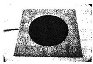
Figure two: wafer raised tray, the vacuum channel below the wafer helps to firmly fix the wafer on the pallet.
Halftone design
Screen board is the most important tool, must be properly designed to achieve high performance rate of outstanding achievements. The role of the stencil is to divide the solder paste into a portion of a finely calculated amount of metallurgical bonding points placed on the wafer. To successfully create a stencil design with flawless results, it is not easy to have high reflow bumps tightly spaced, especially with multiple rows of bare pads spaced below l0um. The mesh cutting technology that affects wafer bumping includes mesh thickness, punch size, shape, orientation and location, and image alignment.
The basic design items that affect the printing effect of wafer bump screen -3
Screen cutting technology
For wafer bumping, the cutting technique must produce thousands of closely spaced, very small perforations with extremely high dimensional and positional tolerances. A slight deviation from the optimum punch size can also cause significant uplift height differences, which in extreme cases lead to chips that have been assembled and bottom packed. In addition, the location of the punch must also be kept accurate as close as possible to the computer generated design. The whole wafer pad must be printed, in order to obtain the reflow convex block size can be accepted, when printed on the pad under the condition of close spacing, the space between the perforation must make enough, avoid bridging defects. Therefore, the distance between the holes should not be less than 3mil (for 3mil thick mesh). In some cases, the perforations need to be offset to avoid fully placed in the center of the pad. Depending on the density of holes in a particular area of the screen, it is possible to print only one part of the pad. Since the pad area of the wafer can be less than 4mil, the stencil cutting technique must be able to accurately locate the hole, and the offset is only less than a few microns.
Of the existing technologies in the market, only laser cutting and electroforming are suitable for copying computer generated drawings and can meet the requirements of effective wafer printing. Although many different vendors use the same technology to cut web boards, their capabilities vary. In general, the laser cutting process leaves a hole through the wall to allow coarse polishing through special polishing and plating techniques. Another feature of laser cutting is that the holes on the screen board are sloped, and the size of the opening on one side of the screen is slightly larger than the other. Some suggestions mean that if the larger punch is at the bottom of the stencil, the beveled perforation can actually increase the stencil release. The disadvantage of laser cutting technology is that the cost of producing a stencil with numerous perforations is higher, and the more the number of perforations, the higher the cost of producing a laser cutting stencil. On the contrary, the original production cost and design of the electroformed stencil perforation is independent of the number, size and location of the electroformed stencil punch and laser cutting board and a perforated wall equally accurate, although not natural cut, but relatively smooth.
Screen thickness
The thickness of the halftone foil plays a decisive role in determining how much perforation is required to coat the amount of solder paste required to reach the target bump height. According to the study of wafer bumping, it is recommended that the thickness of the mesh plate be chosen according to this standard: the ratio of the minimum wall area to the perforated opening area (i.e. area ratio) of the minimum perforation on the screen is less than 1.75.
Perforation size
In the correct stencil design that meets the requirements of less than 1.75 of the recommended area, the thickness of the stencil and the size of the perforation are very closely related. If the required amount of solder paste is the same, a thinner stencil requires a larger punch size; a thicker die requires a smaller perforation size. For closely spaced pads, sometimes the most appropriate combination of perforation size and thickness shall be found to achieve acceptable transfer efficiency. It is a challenging job to meet the requirements of solder paste and not to punch holes too tightly. The biggest screen design challenge is often in the corner of the bare chip, which is common. Another important item we should pay attention to when designing oblique laser cutting holes is: it must be kept in mind that the opening area at the bottom of the screen must be larger than the top, and the opening area is larger, which means the space between the perforations is smaller.
Perforation shape
In the process of screen printing, the filling and releasing steps are affected by the shape of the perforation. To achieve more consistent and excellent quality of packing, the perforation has better effect than the fillet angle, because slightly curved edge flow through the solder paste filling is far easier to fill the sharp corners, and elliptical and circular packing effect is much better than that of triangle and diamond. However, rounding holes have little to do with the release process.
The basic design items that affect the printing effect of wafer bump screen -4
Punch orientation
The size and geometry of the perforation are important considerations when designing a solid mesh plate, but the influence of punch orientation on the size distribution of the reflow bump is not to be neglected. In addition to the transfer efficiency of the highest fill most of the paste, and do not cause excessive collapse caused by defective solder paste bridging, screen printing paste volume make the wafer per chip agreement is also very important. If the height of the bulge formed by reflow solder paste is too wide, it may open or short circuited after assembly. Larger bulges may stick to multiple adhesive pads or other objects: bulges are inadequate and cannot hold any object. By designing a suitable screen plate for punching, the printing accuracy can be improved and the distribution of the solder paste coating can be improved.
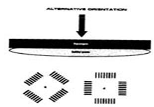
Figure three: the amount of solder paste filling in rows such as A may be inconsistent with the arrangement of perforations such as B.
The circular punch has no directional problem, because the orientation of the object is the same at any angle; but the square is not, and at 45 degrees it turns into a diamond. Oval and rectangular hole is more serious, because the thing north and South orientation, or any directional angle orientation are not the same, screen printing paste filling in different ways of perforation of the same size and geometry, but also have different perforation orientation. To achieve consistent packing and release, it is better to have all the perforations aligned in the direction of the print: however, it is not easy without adding certain techniques into the design.
One way is that all the perforations are perpendicular to each other, such as the punched directional strategy used by standard QFP components. When moving to 45 degrees, all vertical holes are diagonal, as shown in figure 3. Typically, the mesh vendor can move the entire vertically oriented punch mode to 45 degrees, while the wafer must also be moved under the mesh for coordination. In addition, due to the close arrangement of adjacent rectangular and oval holes parallel to each other, so that there is a greater chance of bridging defects, so the adjacent perforation design has helped to reduce the possibility of vertical bridging defects.
The basic design items that affect the printing effect of wafer bump screen -5
Punch location
Standard SMT applications such as QFP or BGA screen printing device, the position of the welding pad central paste coating, but it will be so fresh wafer printing, pad printing but completely block, let the amount of paste to form solder paste height distribution of reflux effectively raised. In very narrow spaces, it is difficult to place holes and pads symmetrically and leave enough space (or at least 3mil) between adjacent perforations to prevent bridging defects. In this case, it is recommended that the solder paste cover at least 50% of the pad so that the solder paste is withdrawn properly and completely coalesced on the pad. In addition, the center (rather than the end) of the perforation is preferred to deviate from the pad in order to make the process ideal, as shown in figure 4.
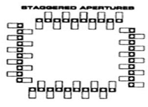
Figure four: the two scenarios in the figure are elongated, elliptical, perforated, offset pads placed in a perforated B, and the solder paste is pulled back to the pad during reflow.
For close spaced pads with single row perimeter arrangement, large-scale coating and bridging avoidance can be a difficult problem. Wafers designed for lead bonding of chip electrical interconnects usually have this configuration. In these cases, the perforations can be made into narrow elongated elongated oval or rectangular geometries and arranged in an interlaced mode to separate the adjacent solder paste as much as possible.
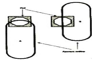
Figure five: for single row pad configurations, an effective method of applying a large number of solder paste on the pad and reducing bridge risk is to stagger the holes.
Fig. 5 is an example of this method, and if the space is abundant, the interleaving arrangement may also be applied to a multi line pad layout. For pads that are near the cut off sheet, a solder paste that does not have any non passivation metal must be employed. There is a very important point, can not be placed on the other is the perforation does not accept the exposed metal parts (such as solder paste characteristics of reference point, mark or trademark), these characteristics may have a serious influence on the validity of this method is raised, and the screen placement process brings great challenges of perforation. In addition, it may be difficult to find enough space for fitting holes in the patch pads at the bare corners. Since the maximum limitation of the perforation characteristics comes from these aspects, it is suggested that the stencil design process be initiated in order to avoid possible catastrophic problems in the downstream process.
conclusion
Screen printing wafer bumping technology is a low-cost solution that can be used to replace conventional processes such as evaporation or electroplating. However, with the I / 0 increase in the number and spacing decreases, in these joints printing paste is becoming more challenging, but also for the use of screen, with matching materials (such as solder paste, screen etc.) and process design standard is greatly improved. Therefore, people continue to carry out research in order to better understand these details, so as to further improve the process of stencil printing.