0512-57906238
Tel:13656269491
Fax:0512-57906239
Mail:mef@micro-ef.com
Addr:No. 189, ZhangJi Road Kunshan City ,China
In the field of surface mount assembly, the stencil is the key to achieving precise and repeatable solder paste coating. As the solder paste is printed through the stencil perforation, the solder paste and glue points of the fixed element position are formed, and the elements are firmly bonded to the substrate during reflow. The composition and design of plate thickness and perforation size and shape - will ultimately determine size, shape and location of the gel point, which is the key technology to achieve high yield at least defects, defects may include insufficient solder or dislocation.
SMT has become the mainstream assembly technology since 80s, and remarkable progress has also been made in halftone technology. Today, vendors can design a mesh using multiple materials and manufacturing technologies to meet the most challenging assembly technology trends: precision spacing technology, component miniaturization, and intensive circuit boards.
In addition, halftone technology is now used in a full range of mass extrusion printing materials. The screen designer has in-depth understanding of perforation size and shape influence on material deposition, prompted the emergence of new technologies (and will continue to emerge, the platform and screen printing) technology into the application field of every kind of, such as adhesive coating and wafer bumping.
The mesh has two main functions, regardless of the material or manufacturing process used. The first is to ensure that the coating material is accurately placed on the substrate, such as solder paste, solder paste or sealant; and second is to ensure that sizing and sizing are suitable.
Halftone material and manufacturing
The most widely used mesh material is metal, mainly stainless steel and nickel. In recent years, a variety of plastic materials have gradually been accepted. Screen manufacturing technologies include chemical etching, laser cutting and electroforming. With a brief look at these materials and processes, it is found that manufacturers can choose from a wide variety of mesh boards to meet specific application requirements.
In the past, the most commonly used low cost stencil fabrication method was chemical etching, a reduction process using lithography to determine the perforation pattern, and then using an etchant to form perforations on both sides of the mesh. In order to obtain the perforation has wall to improve the performance of the ladder can be specially designed solder paste demolding, in the screen side toward the substrate generated larger perforation.
This manufacturing technique has some inherent drawbacks - Double etch, knife edge punching, contour forming, and "less etching" and "over etching". To overcome these defects, electrolytic polishing can be performed to remove the edge of the knife after etching so that the perforated walls become smooth. Chemical etching applies to large perforation / coarse pitch applications, but does not meet the requirements of today's 0.5mm below spacing applications.
In order to meet the requirement of fine pitch and improve the density of components, laser cutting has become a more widely used stencil manufacturing process. The laser cutting stencil can be directly generated from Gerber data (or other format data) without the need for multiple photolithography steps. This significantly reduces the chance of image dislocation. CNC (CNC) laser cutting is directly driven by Gerber data to generate highly accurate repeatable stencil punched holes. This precise technique allows the hole size to reach + 5 microns, even under large printing areas.
The laser itself is a unique flexible tool. By adjusting the intensity of the laser in the manufacturing process, a high contrast reference can be generated on the surface of the stencil without filling. What's more, this feature helps to improve the accuracy of the manufacturing process. With the inherent characteristics of this process, a perforated cross section with trapezoidal cross section can be produced to improve the release of solder paste. But some people worry that the laser will leave a unique "fine stripe" surface on the perforated wall (Figure 1).

Figure 1: laser cutting holes have special stripe markings
The new laser cutting technology has this stripe minimized, however, if the specific application needs the hole wall surface is smooth, can use the electronic polishing method, even in the process of electroplating punch cutting and laser cutting.
In contrast to chemical etching and laser cutting, the electroforming process is an addition process in which the electroformed mesh is electrodeposited by electroplating on a mandrel". The electroplated material is usually nickel, and the mandrel has a negative pattern of photoresist with a perforated pattern. This process produces very sophisticated, smooth bore perforations with natural taper and eliminates the need for additional finishing. This very sophisticated process produces an electroformed stencil suitable for ultra precision spacing applications.
In the past five years, the use of plastic as a screen material has attracted considerable attention. At the same time, it has been proved that the standard SMT board can be made from polymer foil and applied to offset printing brush. This kind of material has been accepted by people. The main advantage of using plastics is that they can be made into panels with a thickness of at least 8mm, enabling new process technologies.
To make this kind of screen using standard CNC processing technology, different sizes of the drill perforation preparation on plastic substrates, can use a single thickness stencil printing in a single stroke, adhesive glue dot printing with different height (Figure 2). Very high thickness is also allowed to be excavated, cut and arranged at the bottom of the screen to fit the elements that are pre placed and bent (Fig. 3).
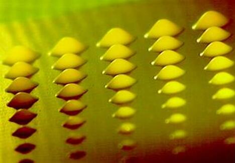
Figure 2: a series of adhesive dots can be generated with a single thickness plastic screen
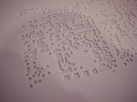
Figure 3: the bottom side of the plastic mesh plate has a cut and cut shape that fits with the components on the circuit board.
Design guidelines and capabilities
The size and shape of the stencil determines the volume, consistency, and shape of the material applied to the substrate. Therefore, strict control of perforation quality is critical to the success of the stencil design, especially for fine pitch and ultra fine pitch applications requiring very precise coating of very small amounts of material. You can use the wall to wall ratio (the opening area divided by the hole wall area) and the aspect ratio (the opening width divided by the mesh thickness) and other parameters to determine the appropriate size of the perforation.
For qualified solder paste release performance, the general criterion is that the wall to wall ratio shall be greater than 0.66, while the aspect ratio shall be greater than 1.5. According to the design criterion of perforation, need to consider a variety of features, such as screen manufacturing technology, for the chemical etching process, it is difficult to achieve the following 1.5 aspect ratio; and the laser cutting and electroforming process of manufacture of 1:1 screen aspect ratio perforation.
The wall is more important than the stencil designer, which is directly related to the final release of the solder paste. In printing, surface tension in the opposite direction occurs when the screen plate is separated from the substrate. These forces determine whether the solder paste goes into the pad to be printed or is still glued to the perforated wall of the stencil.
If the pad area exceeds 66% of the surface area of the perforated wall, the possibility of achieving effective solder paste transfer will be increased. As the ratio drops below 66%, the solder paste transfer efficiency will decrease and the quality of printing will become unstable. Naturally, the smoothness of perforated walls affects these levels of efficiency. Electropolishing and / or electroplating of laser cutting holes in the manufacturing process has been shown to improve the transfer efficiency of solder paste. Similarly, the smooth perforation wall formed by the electroforming process can also improve the stripping efficiency of the solder paste.
Component spacing and punch density are also considerations for selecting the right manufacturing technology. For applications whose spacing is less than 0.5mm, the range of selection is limited to laser cutting or electroforming. Although the two methods have their own advantages and disadvantages, they can produce high quality and high precision precise screen.
The laser process does not require drawings, thus reducing the mismatch problem. Although the thickness of the inventory screen is limited, the laser cutting range can range from 50 to 500 microns. In contrast, the thickness increment of the electroformed stencil can be controlled to be 2.5 microns, and the overall thickness range is from 25 to 300 microns. The electroforming hole method can accurately copy the photoresist surface of the core axis without further processing. However, for ultra precision applications, laser cutting holes may need to be further processed to smooth the perforated walls.
Finally, the number of perforations is also a decisive factor. Laser cutting is a serial process, so the number of holes increases and the manufacturing time increases, which affects the final cost of the stencil. Electroforming can form all perforations in one process, so the number of perforations has little effect on cost. This allows the electroforming process to become a technology for high-density applications such as wafer bumping, but the number of holes used in wafer bumping is about 2 million!
Extended function
Application of plastic materials to increase the screen stencil design personnel available types of instrument further, in the top screen manufacturing step and surface arrangement in a perforated bottom plate, this is the latest progress in extending the basic function of screen printing technology. Depending on the nature of the material, i.e., its viscosity and flow characteristics, perforations with different sizes and shapes can be produced for the production of adhesive dots of different sizes.
The second extension is a closed print head that prints a variety of material onto the substrate through a stencil. Because the material is completely enclosed in the printing system, there is no need to consider material delivery, drying, moisture absorption and waste.
These two advances have enabled the stencil printing process to be added to the assembly process as needed, before or after attaching different types of components. As a result, almost all electronic assembly materials can be used with a properly designed stencil, coated on a bare substrate or placed on a substrate of some components, at a much faster rate than the most advanced dispensing equipment. A horizontal movement of the print head on the screen can fill any number of perforations, even if the maximum I/O number does not cause bottlenecks in the high-speed, high-volume assembly line.
The process itself is inherently flexible because the basic equipment platform is the same. Simply by changing the stencil or using a closed print head, the screen press can be used for coating solder paste, adhesive, flux, sealant, or thermal interface material as needed.
wafer bumping
Wafer bumping is one of the most demanding applications in the most attractive advanced stencil printing applications. In this process, standard stencil printing is used to print solder paste directly on silicon wafers (Figure 4). In order to obtain the desired height of the projection, you need to be printed onto the wafer bonding solder pad. During subsequent reflow soldering, the solder paste is pulled back to the wetted pad surface to form a solid solder bump structure.
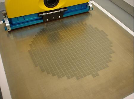
Figure 4: using 110 square microns perforated, with 150 micron spacing on the wafer
Direct printing solder paste points, in subsequent reflow processes, solder paste will be pulled back to the wafer bonding pad to form a single solder bump.
Although the technology may seem simple, it requires extreme control to implement ultra precision processes. The correct stencil design is the key to the whole process. However, design and manufacture of excellent screen perforation, no defective printing results after reflow, the height distribution raised to meet the stringent requirements, it is not trivial, especially for the full array of pad spacing is less than 250 microns.
For wafer bumping, the cutting technique must be able to produce thousands of very small, closely spaced perforations, and Fu Heji requires strict size and positioning errors. For optimum design, slight offset of the punch causes a large bump height change, which, in extreme cases, causes the assembly chip to open.
It is also important to make the location of the perforation as close as possible to the design drawings generated by the computer. Because the entire wafer pad must be printed, in order to obtain the reflow raised qualified size, were printed on fine pitch pads when the perforation and accurate positioning in between there is enough space is very important, and will not produce bridging defects. According to the rule of thumb, the perforation width should not be smaller than the stencil thickness to reduce bridging defects.
Sometimes, the opening of the punch needs to be offset and not directly aligned with the pad. Depending on the perforation density of the particular area of the screen, it may be necessary to print only part of the pads. When considering the wafer pad size may be less than 100 microns, mesh cutting technology can precisely locate hole opening is very important, offset can only be biased in one aspect, a few microns.
In designing stencil punching, the usual method is reverse design from wafer scale. According to this information, the volume of the solder paste can be calculated and then used to design the size of the perforation. At this stage, it is necessary to fully understand the perforation wall to wall ratio effect. Ideally, the largest perforation of the thinnest mesh sheet with the largest perforation spacing can achieve the optimum process, but there is an unavoidable tradeoff.
According to extensive research, the generation of solder paste transfer efficiency curves can provide assistance for screen designers. The efficiency of solder paste transfer is shown in Figure 5 relative to the perforation surface wall ratio and the reflow bump planarity. This chart clearly shows that the wall to face ratio must exceed 0.6 in order to achieve process repeatability. With the increase of the wall to wall ratio, the whole process will become more stable.
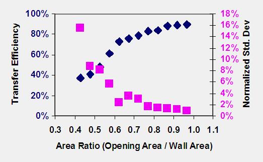
Figure 5: the solder paste transfer efficiency is related to the perforation wall to wall ratio, and affects the planarity of the reflow bump.
The design of a wafer bumping board is a highly skilled work involving a number of parameters that influence each other, such as stencil thickness, punch size, shape, and other factors, including the orientation and positioning of the process. Designers need to understand all aspects of the process in order to provide the best stencil products. With the industry to use the 300mm wafer spacing is reduced to 120 micron, wafer bumping process will further challenge to screen technology. (figures 6 and 7)
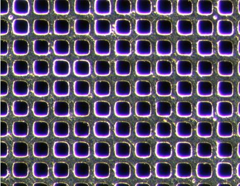
Figure 6: the latest wafer projection board for 300mm wafers holds about 2000000 perforations!
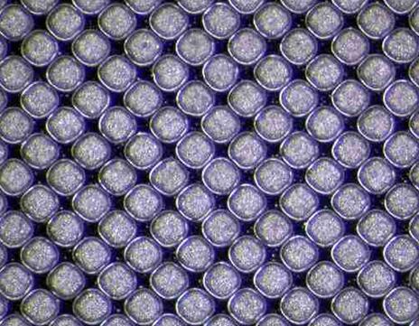
Figure 7: close-up view of the mesh shown in Figure 6, with a hole area of 110 square microns and a distance of 150 microns.
Looking into the future
At present, the board design and manufacturing technology has been developed to meet the standard and precision SMT assembly two requirements, and this trend will continue in the foreseeable future. One challenge in the SMT field is the increasing use of a wider range of hybrid components, so large and small materials are needed to be applied. In response to this trend, mesh vendors need to explore new ways to break the current wall to wall ratio guidelines.
However, the wafer bumping process will pose the biggest challenge to the stencil technology in the coming year. Now there are already more than 2 million perforations! And today's most advanced application is to use 150 micron spacing on 300mm wafers, according to the international semiconductor technology blueprint, which will fall to 80 microns by 2007.
The factors involved in this need include manufacturing capability, pattern alignment accuracy, and pattern stability. The present material is likely to have reached its limit. In order to achieve less than 100 micron pitch, manufacturers of vision may need to develop new plate materials and manufacturing technology, in other words, the latest chapter in the development of screen technology has yet to be written, please wait.